Input Devices
Tapas Ranjan Barik
Individual Assignment
Measure something: add a sensor to a microcontroller board that you have designed and read it.
Group Assignment
Probe an input device(s)'s analog and digital signals
Individual Assignment
In computing, an input device is a piece of equipment used to provide data and control signals to an information processing system such as a computer or information appliance. Examples of input devices include keyboards, mouse, scanners, cameras, joysticks, and microphones.
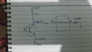
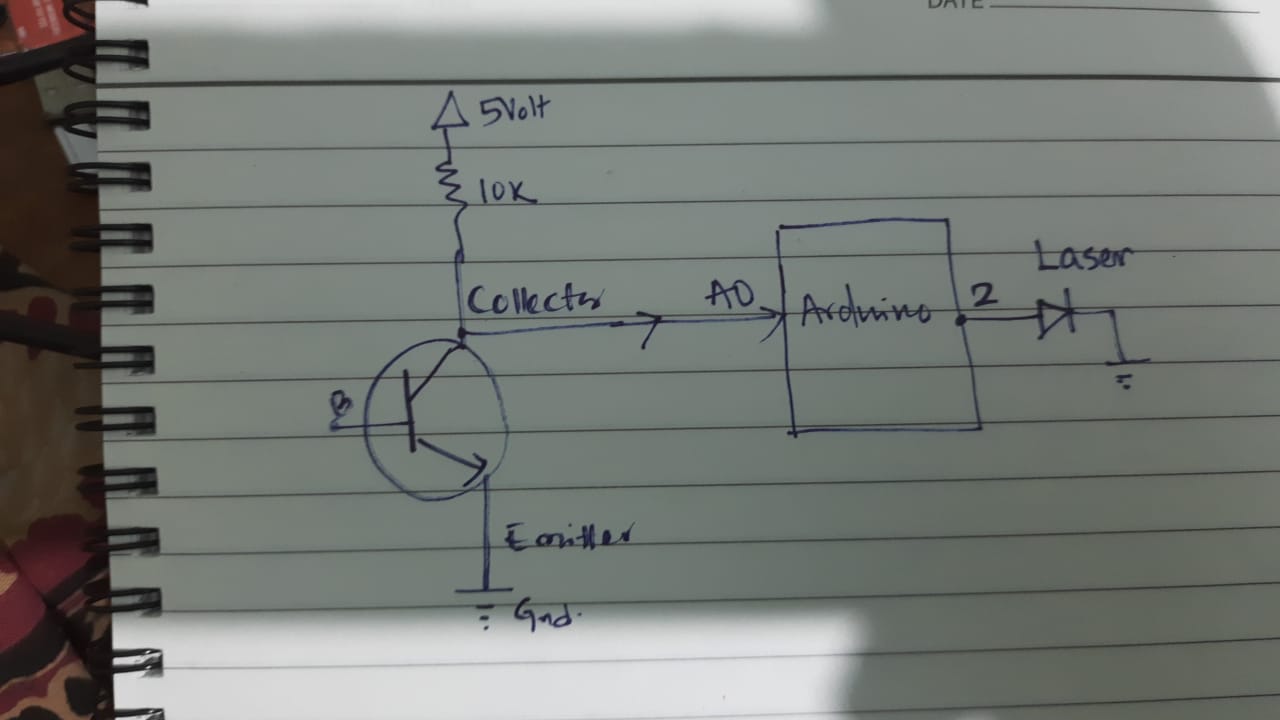
In this week i have design,implement and test input of the leaser sensor with photo transistors in my final project i have to make IoT BASED IV DRIP MONITORING where i have to count the drip of IV. Here i have taken photo transistors which using as input for detecting of IV drop
Phototransistors
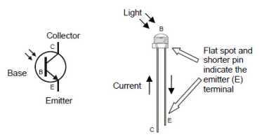
A Phototransistor is a
semiconductor device that is sensitive to light. It alters the current flowing between the emitter and collector, according to the level of
light it receives. They are similar to a regular transistor except that it has a light-sensitive Base terminal. The base-collector junction of
the phototransistor is also larger as it is the light-sensitive region of the sensor.Phototransistors are a form of bipolar transistor that is sensitive to light - having the gain of a transistor they are much more sensitive than photodiodes.
Generally, in the case of phototransistor circuits, the collector terminal will be connected to the supply voltage and the output is obtained at the emitter terminal while the base terminal, if present, will be left unconnected. Under this condition, if light is made to fall on the base region of the phototransistor, then it results in the generation of electron-hole pairs which give rise to base current, nothing but the photo-current, under the influence of applied electric field. This further results in the flow of emitter current through the device, resulting in the process of amplification. This is because, here, the magnitude of the photo-current developed will be proportional to the luminance and will be amplified by the gain of the transistor leading to a larger collector current.
The output of the phototransistor depends on varies factors like
- Wavelength of the incident light
- Area of the light-exposed collector-base junction
- DC current gain of the transistor.
Advantages of Phototransistor
The advantages of phototransistors include:
- Simple, compact and less expensive.
- Higher current, higher gain and faster response times in comparison with photodiodes.
- Results in output voltage unlike photo resistors.
- Sensitive to a wide range of wavelengths ranging from ultraviolet (UV) to infrared (IR) through visible radiation.
- Sensitive to large number of sources including incandescent bulbs, fluorescent bulbs, neon bulbs, lasers, flames and sunlight.
- Highly reliable and temporally stable.
- Less noisy when compared to avalanche photodiodes.
- Available in wide variety of package types including epoxy-coated, transfer-molded and surface mounted.
The applications of phototransistors include:
- Object detection
- Encoder sensing
- Automatic electric control systems such as in light detectors
- Security systems
- Punch-card readers
- Relays
- Computer logic circuitry
- Counting systems
- Smoke detectors
- Laser-ranging finding devices
- Optical remote controls
- CD players
- Astronomy
- Night vision systems
- Infrared receivers
- Printers and copiers
- Cameras as shutter controllers
- Level comparators
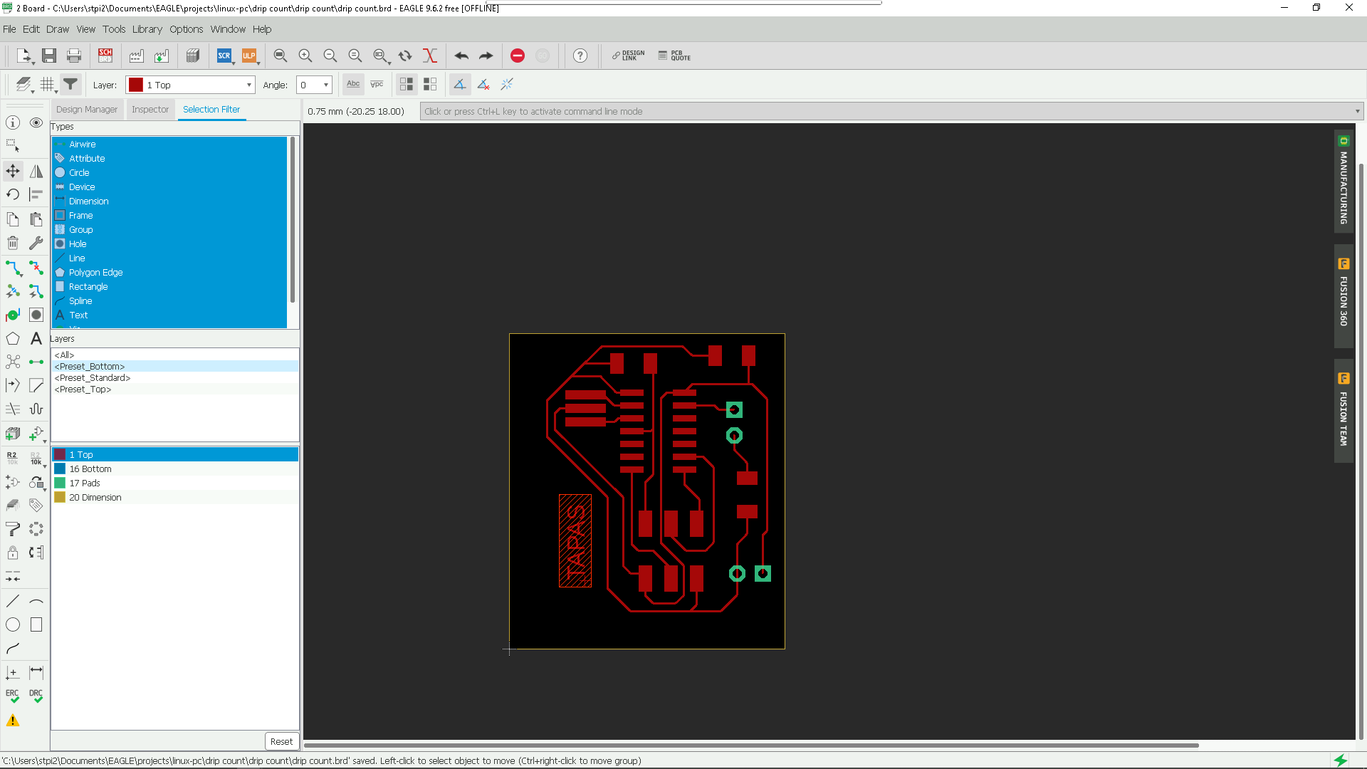
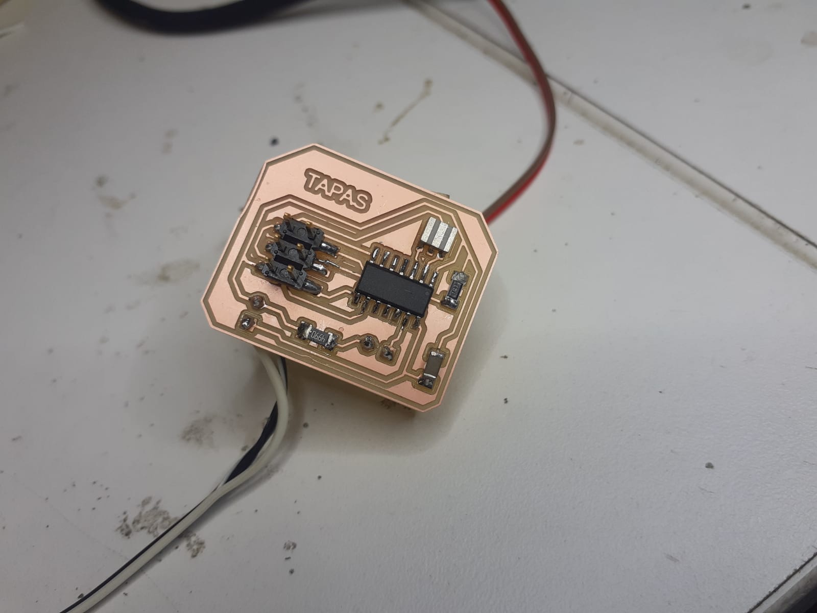
PCB Designing
For designing the PCB circuit I used AUTODESK EAGLE.
I used ATtiny44 as the microcontroller,
Here i use fab 6 pin header as just as six pind header, i will connect 3 pin for leaser module and 3 pin for phototransiter
I can use this same board for my final project
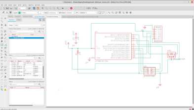
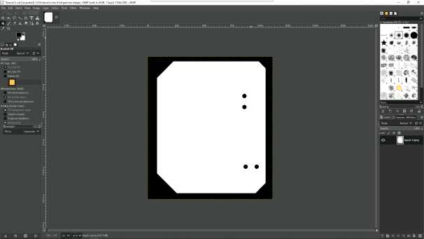
Change the design rule. Electronics Production Then I arranged the components to obtain the board circuit

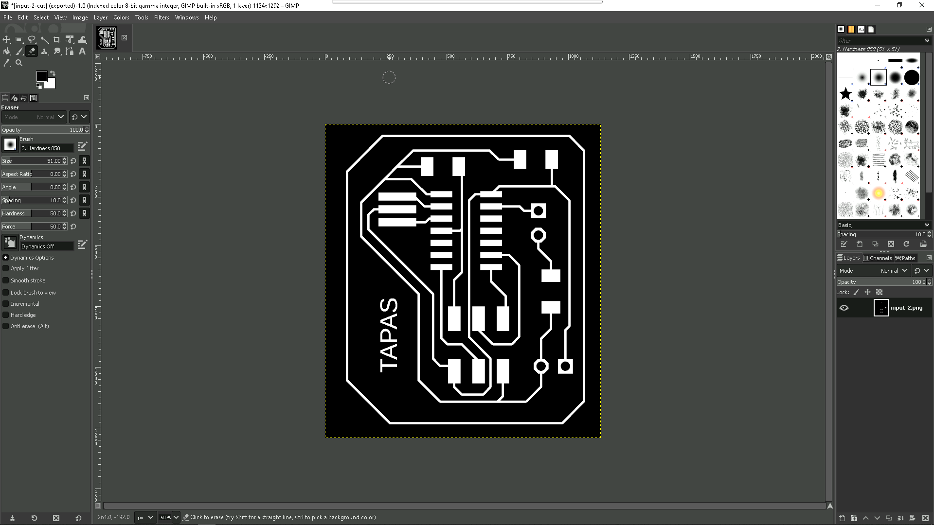
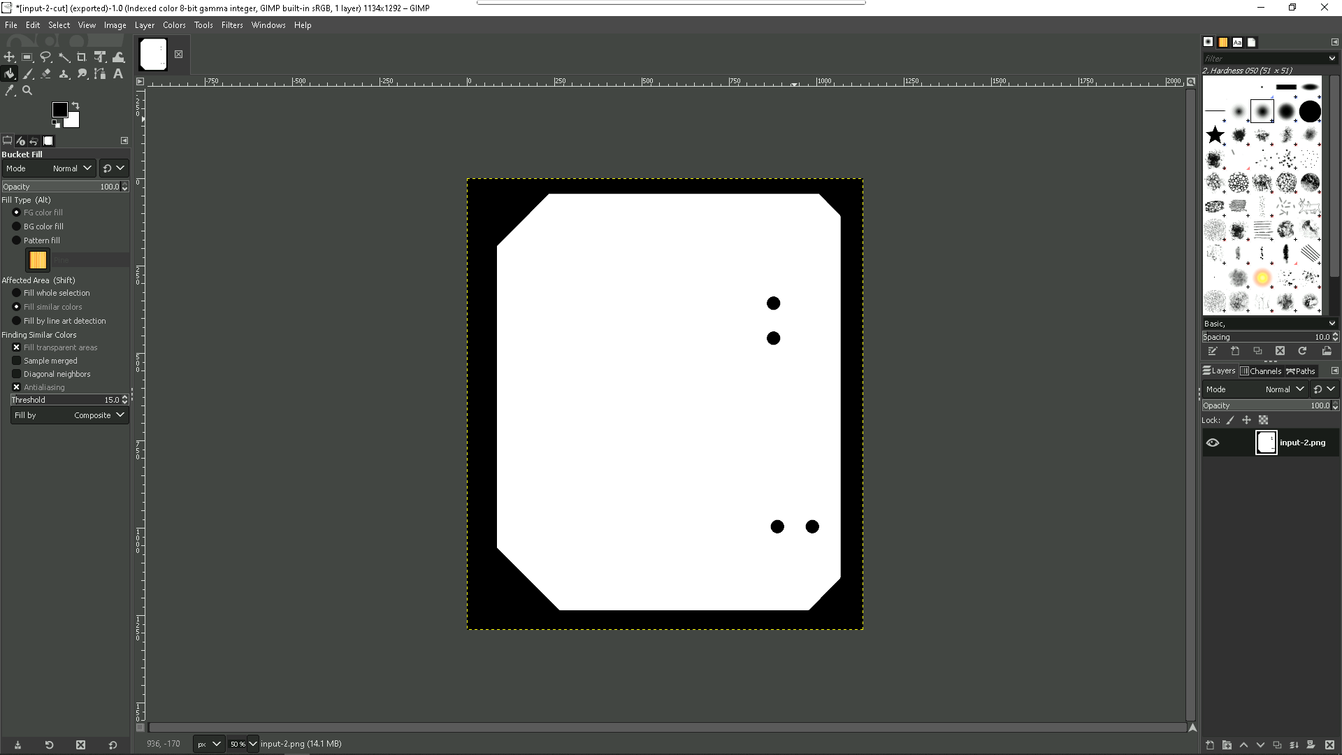
Following are the trace and cut file for the ckt bord
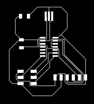

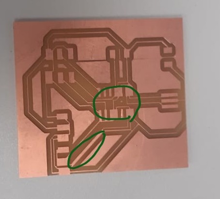
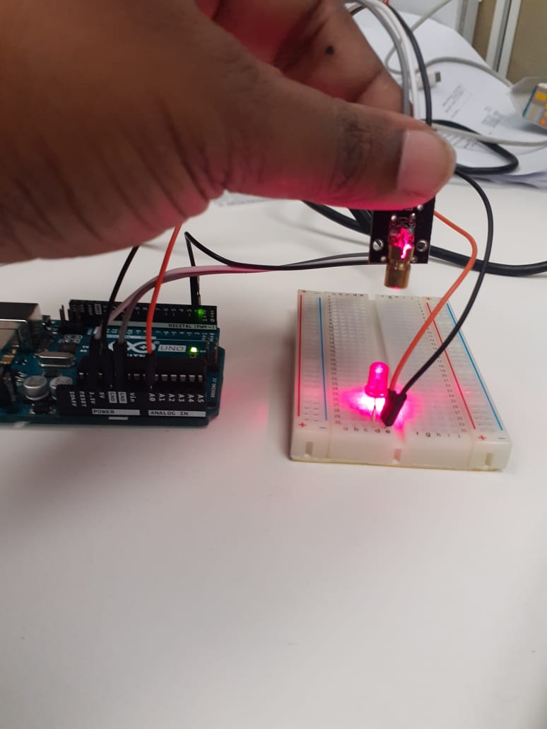
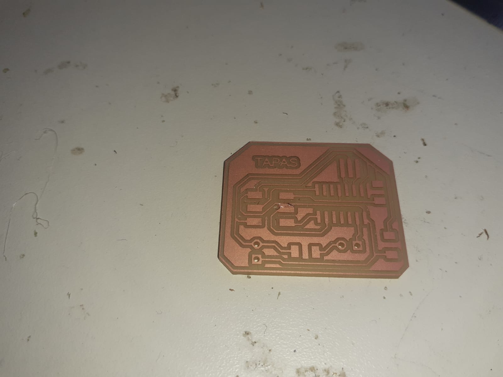
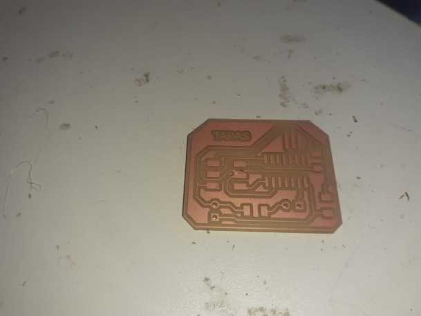
The PCB is not properly cut its path is not cut hence i have not solder the PCB i use Arduino and breadboard for testing
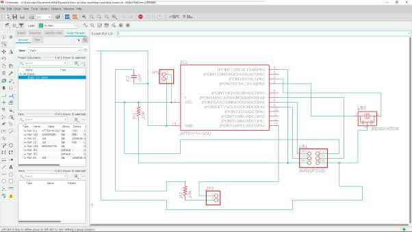
I have to rework on the designing of my pcb.


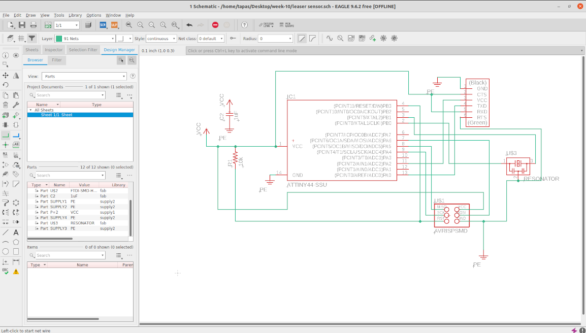
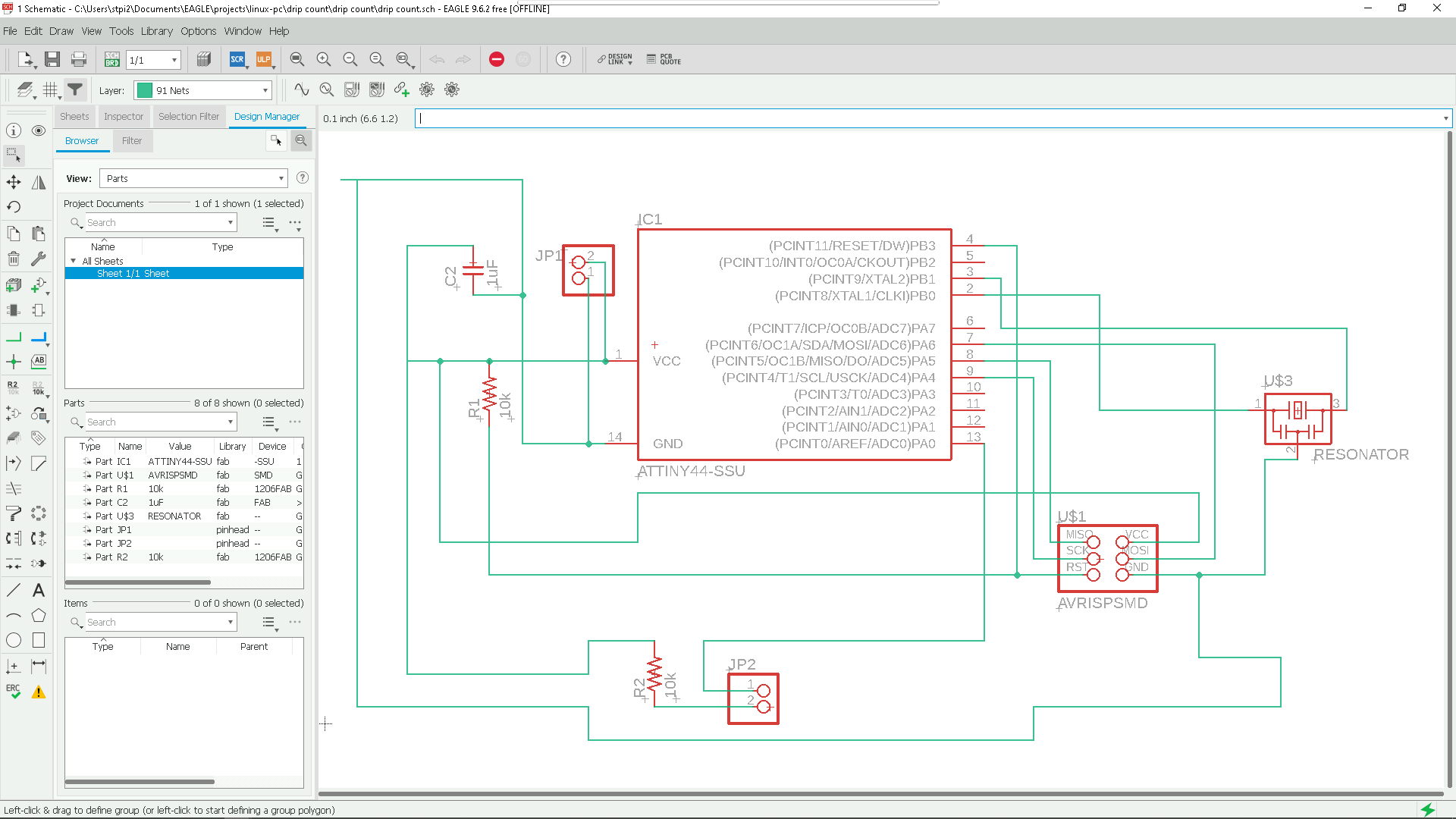
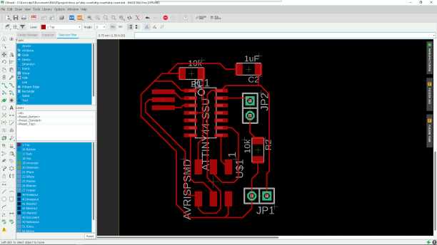
schematic diagram
In this week last above pcb is not pinted correctly due to wrong DRC and routing hence i have rectified as below here in this schematic i have taken PA0 as input to JP2 is connected Photo transistor and leaser diode is connected n jumper JP1
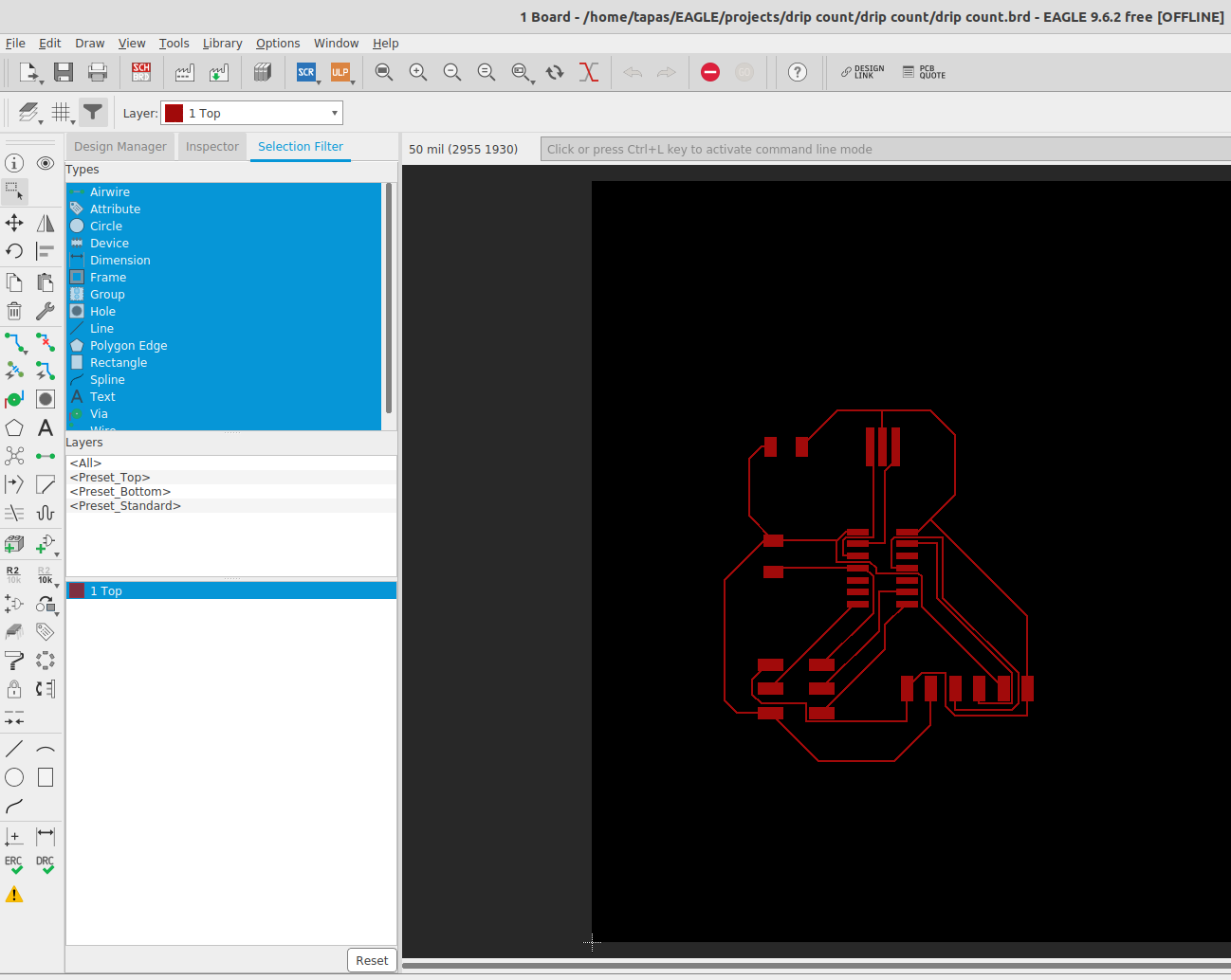
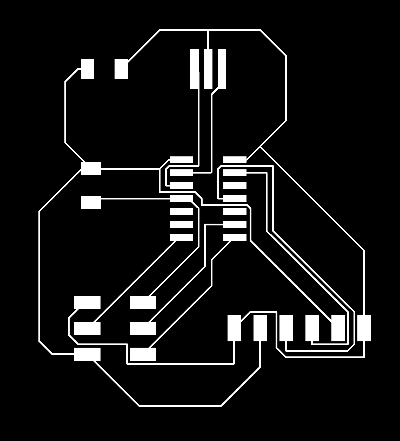
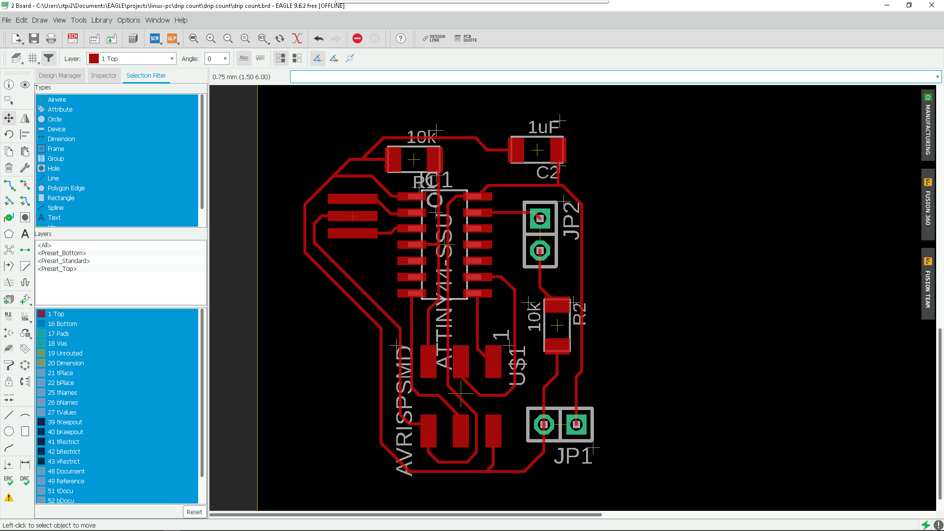
PCB Routing
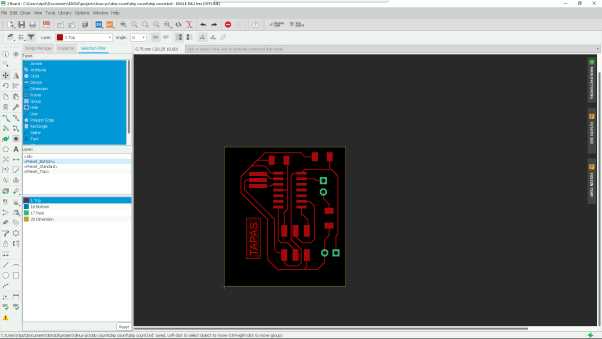
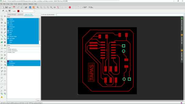
PCB Trace
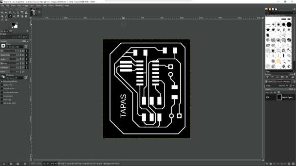
PCB Cut
PCB Print and Soldering

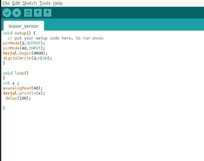
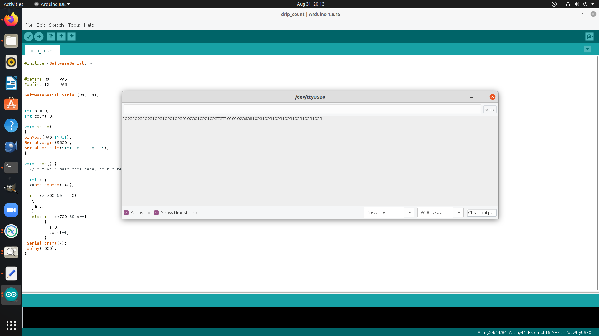
Testing
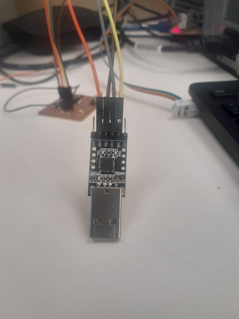
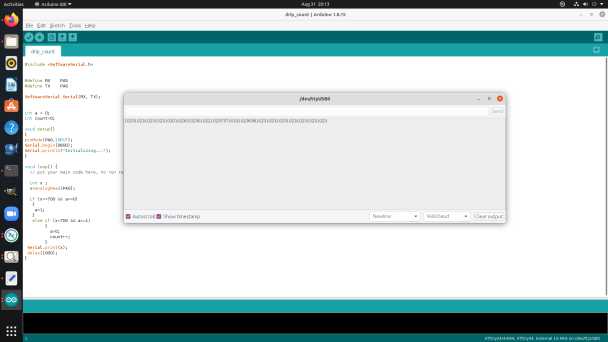
ATtiny chips do not have direct support for hardware based serial and therefore the Serial object is unavailable in your code, however,
it is easy to add a SoftwareSerial object and view output in the Arduino IDE.
The Software Serial library is straightforward to use. Start by ensuring the include statement is specified near the top of your sketch. Next, create a SoftwareSerial object specifying the RX pin (pin to receive on) and the TX pin (pin to send on) when creating the instance
Click to download the file :
Resources:-
https://www.electrical4u.com/phototransistor/
https://circuits-diy.com/what-is-a-phototransistor-basic-electronics/
https://www.instructables.com/How-to-Use-Arduino-As-USB-to-TTL-Serial-Converter-/
https://iot-guider.com/ftdi-usb-to-ttl/programming-using-ftdi-usb-to-ttl-serial/
https://www.hackster.io/porrey/easy-serial-on-the-attiny-2676e6
In this week i have design,implement and test input of the leaser sensor with photo transistors in my final project i have to make IoT BASED IV DRIP MONITORING where i have to count the drip of IV. Here i have taken photo transistors which using as input for detecting of IV drop
The output of the phototransistor depends on varies factors like